Executive Summary
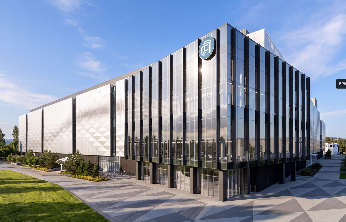
- •Applied Materials opened a $5B shared R&D facility in Silicon Valley to collaborate with TSMC, Intel, and Samsung on advanced chip manufacturing.
- •The 600,000-square-foot site contains almost four acres of cleanroom space and targets a 30% reduction in chip development lifecycles.
- •Engineers will work in parallel to co-optimize 3D architectures and hybrid bonding before the technology reaches commercial fabs.
Community Sentiment
Key Developments & Data
Zubiqo Strategic Assessment
Primary Impact
Hardware manufacturers, semiconductor equipment vendors, and AI infrastructure developers who rely on advanced packaging and 3D architectures to scale compute capacity.
Strategic Shift
Transitioning from siloed, sequential chip design pipelines to parallel, cross-industry R&D to match the rapid development cycles of frontier AI models.
The Ripple Effect
If the facility successfully cuts development cycles by 30%, fabs will receive pre-optimized equipment, accelerating the ramp-up to high-yield production for trillion-transistor packages by 2030.
This intelligence assessment is generated by Zubiqo's AI for informational purposes only.
Intelligence Quality Rating
Grade this brief: Slide & release to submit rating, or tap a preset.
The daily signal, delivered every weekday.
A concise weekday briefing on AI, technology and business. Zero PR fluff.
Subscription completes on Substack • Free • 1-click unsubscribe anytime

:quality(82)/ee08314885c84a6b8c6a25179c2ec0fe)