Executive Summary
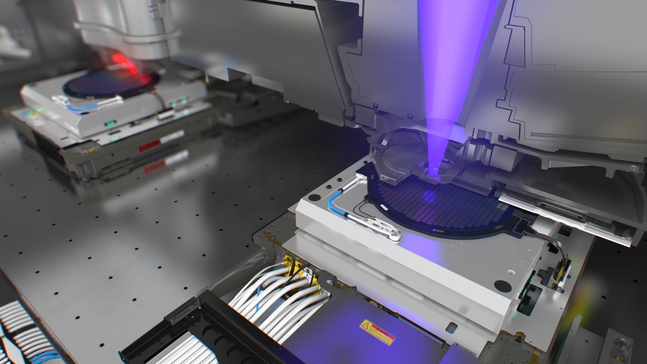
- •Intel surpassed one million 300-mm wafers processed on High-NA EUV tools.
- •Production jumped from 30,000 wafers in February 2025 to over 1M by September.
- •The company is pushing for larger 6x12-inch photomasks to eliminate costly field stitching.
Community Sentiment
Key Developments & Data
Zubiqo Strategic Assessment
Primary Impact
The global semiconductor lithography supply chain, specifically mask blank manufacturers, inspection tool vendors, and ASML's future scanner roadmap.
Strategic Shift
The transition from conventional 0.33-NA scaling to 0.55-NA EUV production, highlighting the physical limits of current 6x6 reticles and the massive capital cost of field stitching.
The Ripple Effect
Intel's insistence on 6x12-inch masks will likely force ASML and peripheral toolmakers to alter their long-term roadmaps, potentially delaying competing foundries that rely on the older stitching standard.
This intelligence assessment is generated by Zubiqo's AI for informational purposes only.
Intelligence Quality Rating
Grade this brief: Slide & release to submit rating, or tap a preset.
The daily signal, delivered every weekday.
A concise weekday briefing on AI, technology and business. Zero PR fluff.
Subscription completes on Substack • Free • 1-click unsubscribe anytime